PLEASE NOTE: If you had an account with the previous forum, it has been ported to the new Genetry website!
You will need to reset the password to access the new forum. Click Log In → Forgot Password → enter your username or forum email address → click Email Reset Link.
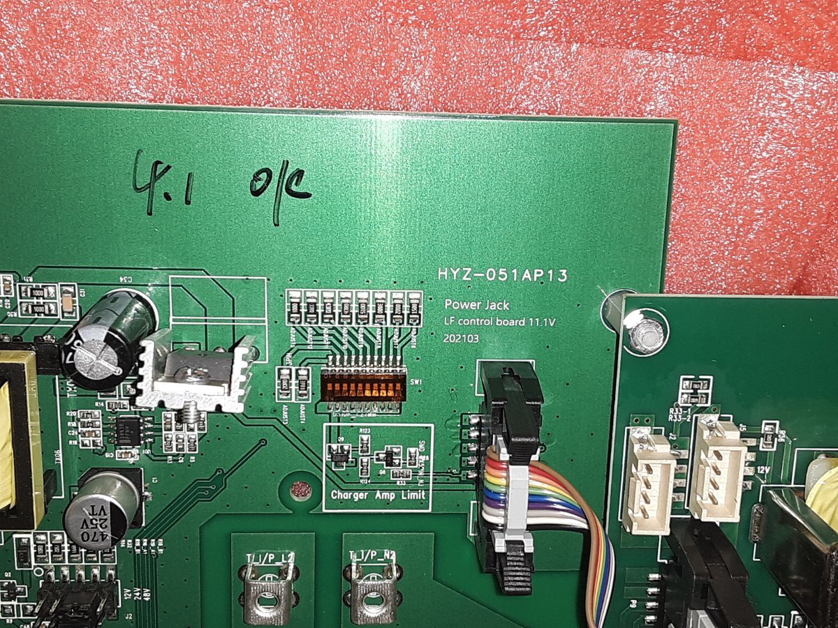
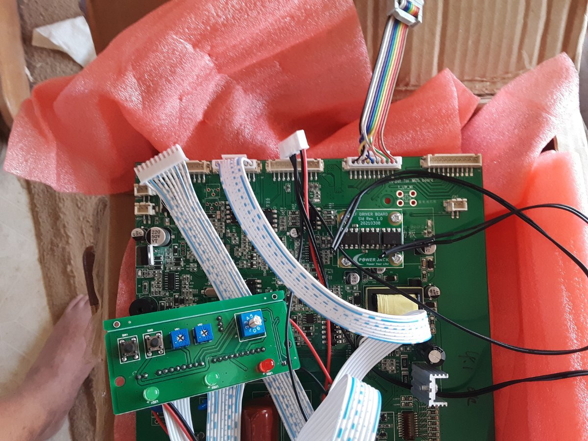
The upgrade board arrived.
Whole Board
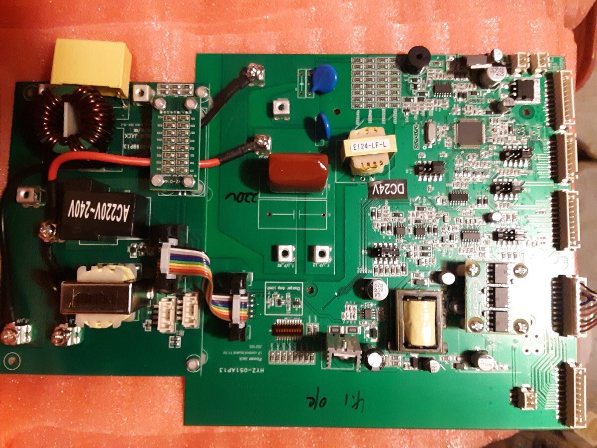
Driver board.
Here's the control 'panel'.
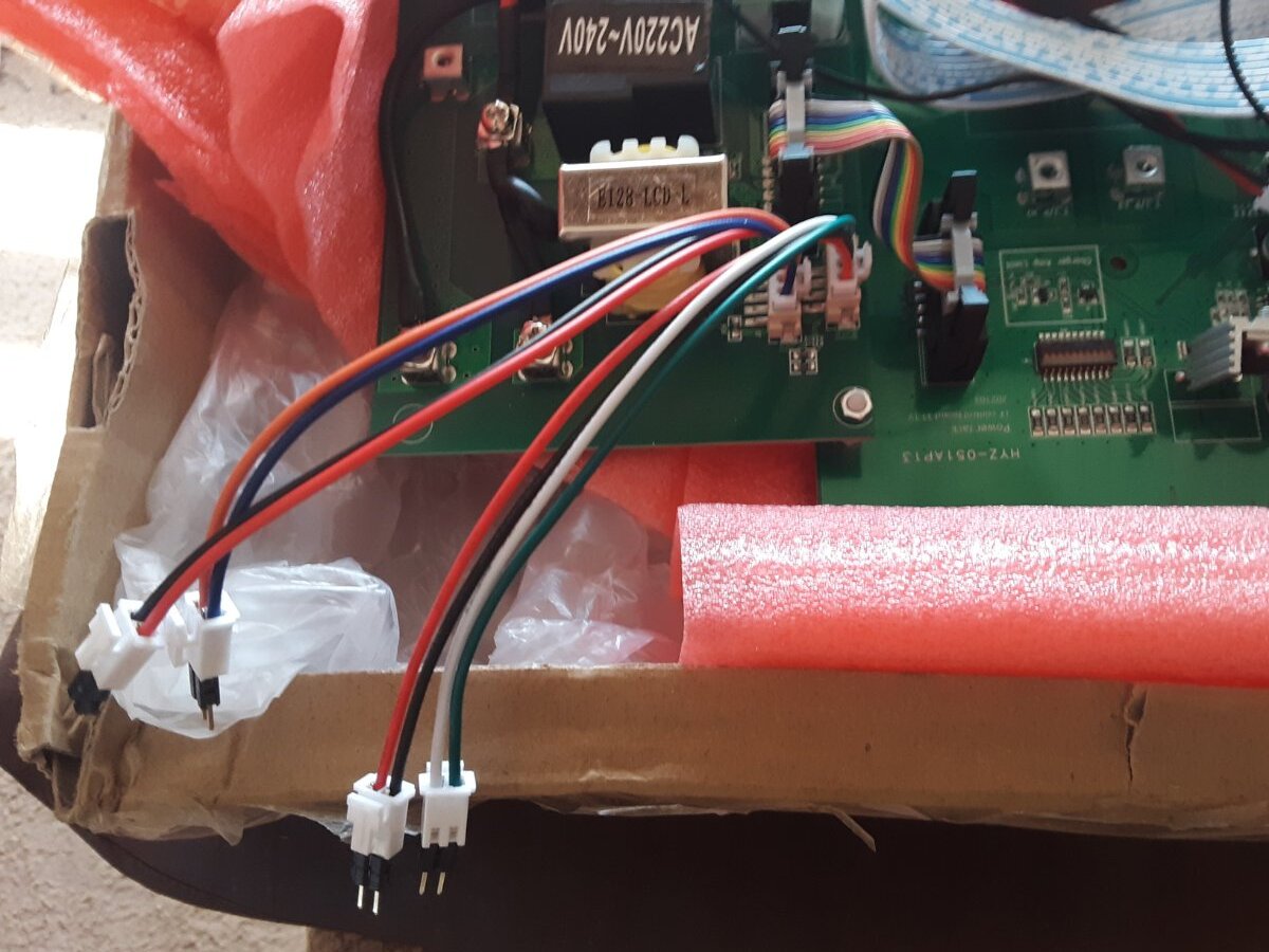
The board has three open 10pin sockets, and the wire harness has two 10pin plugs. I do not know what goes where. I'm not sure ehe rainbow colored ribbon will be long enough to plug into the 'sub-board'. My existing ribbon is much longer.
You can also see the two thermistors.
As for the control board, I'm going to need to drill some holes and nibble the square. I will also need some standoffs - preferably plastic.
I believe the standing rotary switch is the Charge Rate Switch. I have know idea what the others do.
I think these go the fans ???
Here's the charger version
Thar be the underbelly of the beast.
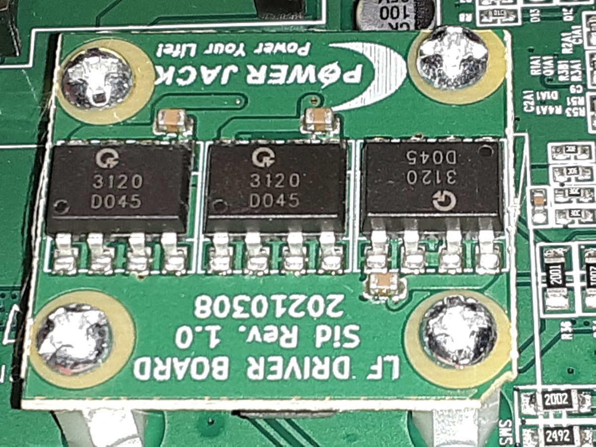
The 3rd photo from the top is Sid Rev. 1.0 LF Driver Board . Is this LF board from Sean and Sid or is this from Powerjack in China ? I have a 11.1 control board but do not know how to connect to the main board as the mainboard connector is different from 10.3 control board . No help from China .
The 4th photo from the top is really confusing as the red and black sensor connector go the center of the 11.1 control board . The sensor connector go to the left end on the 10.3 board . The mainboard ribbon connector go to the right side where the wire is twisted on the 11.1 board . The ribbon cable to the 10.3 is straight and not twisted . Is this the re design of the new powerjack inverter ? I can not get any 10.3 or older powerjack parts . Any comment ?
11 minutes ago, dickson said:Is this LF board from Sean and Sid or is this from Powerjack in China ?
Funny, after telling me that it blew FETs up at higher wattages, they shipped at least several out. This is a board design I provided to them as a drop-in-replacement for their LF Driver board, but only it's perfectly balanced...
I haven't gotten one on my bench to see what causes the problem, but I suspect it's EMI on the ribbon cable punching through the FET gates...
1 hour ago, Clark said:As for the control board, I'm going to need to drill some holes and nibble the square. I will also need some standoffs - preferably plastic.
Shouldn't need to; the mounting holes for the control board have never changed (to my knowledge). Should be able to use the old standoffs.
<img class="ipsImage ipsImage_thumbnailed" data-fileid="459" data-ratio="75.00" width="300" alt="image.png.dc3b92276ad8bd2ea3bca84472ec5fd0.png" data-src="/monthly_2021_06/image.png.dc3b92276ad8bd2ea3bca84472ec5fd0.png" src="/applications/core/interface/js/spacer.png" />
These connectors are intended as plug-in upgrades for your v7 LCD board (if your inverter had one); these are the AC output voltage and current feedback lines, as well as +12v for powering the LCD board.
It does appear that the round current transformer is missing from this, or else you're expected to have one from the old board...
1 hour ago, Clark said:I believe the standing rotary switch is the Charge Rate Switch. I have know idea what the others do
Standing rotary switch is something like that...some preset charge programs, some of which are higher than the overvoltage shutdown. Go figure!
The 2 buttons switch between 50/60Hz, and "speaking language" (but curiously they didn't provide the voice chip on your front panel board...)
One knob adjusts the battery voltage feedback to the CPU (changing every single setpoint), the other adjusts the AC voltage feedback to the CPU.
1 hour ago, Clark said:The board has three open 10pin sockets, and the wire harness has two 10pin plugs. I do not know what goes where. I'm not sure ehe rainbow colored ribbon will be long enough to plug into the 'sub-board'. My existing ribbon is much longer.
Go Power Jack...
I told 'em that the ribbon cable is too thin for the driver current. They concluded that the ribbon header couldn't handle 22 AWG wire, so they switched it to a 10-pin XHB connector--and then stayed with the ribbon cable wire, which is part of the problem all along...
SO...the 10 pin cable from the front panel board goes to the CENTER 10-pin connector. The connector with the thermistors, etc. goes in the LEFTMOST 10-pin connector (with the two 2-pin 12v fan connectors below it).
The rightmost 2 10-pin connectors (near the LF Driver) are the FET drive signals. They sure made life hard for you with that board...
SO...the 10 pin cable from the front panel board goes to the CENTER 10-pin connector. The connector with the thermistors, etc. goes in the LEFTMOST 10-pin connector (with the two 2-pin 12v fan connectors below it).
The black and red wire connector go to the left and this is the same as the 10.3 control board . The 11.1 and the 10.3 board is the same except why PS send the LF Driver Rev. 1.0 that you design . Will the FET blow out on 15kw inverter but not his 8kw inverter ? Maybe PS make more money by selling parts .
WOW... Lots of good stuff.
Here's my original post with pics of my 2016 (or 2017??) version 7 Power Jack.
<iframe allowfullscreen="" data-embedauthorid="71" data-embedcontent="" data-embedid="embed3239521875" scrolling="no" style="height:257px;max-width:502px;" data-embed-src="/topic/157-version-110-control-board-for-my-old-version-7-powerjack/?tab=comments&do=embed&comment=2743&embedComment=2743&embedDo=findComment#comment-2743">
2 hours ago, dickson said:Is this LF board from Sean and Sid or is this from Powerjack in China ?
The website I purchased the 11.0 board is https://powerjackpowerinverter.com/ Took ten days to get here Fedex from china.
2 hours ago, Sid Genetry Solar said:the mounting holes for the control board have never changed (to my knowledge)
I meant the voice/voltage/hertz/Whatever board. My 7.0 only has the one rotary switch for charging voltage on the front next to the power switch.
So... connecting the VVHW (voice/voltage/hertz/Whatever) board to the control board:
VVHW CN2_1 connects to control board CN1_2
VVHW CN2_2 connects to control board CN1_1
VVHW CN2_3 (2pin,red/black) connects to control board CN3 with the thermistors.
19 minutes ago, dickson said:Will the FET blow out on 15kw inverter but not his 8kw inverter ?
WHAT?? This has been mentioned several times now...
2 hours ago, Sid Genetry Solar said:The connector with the thermistors, etc. goes in the LEFTMOST 10-pin connector
I was going to ask where do I attach the terms? I only have one on my 7.0 rig on my transformer.
VVHW CN2_1 connects to control board CN1_2
This appears correct when compared to a 10.3 board I have here.
I was going to ask where do I attach the terms?
Temps, you mean? They normally put one on the MOS boards, and one on the transformer. According to my tracing, the leftmost thermistor connection is "MOS", and the right-er one is "trans."
WHAT?? This has been mentioned several times now...
No idea. Your photos are the very first time I've seen my designed LF Driver board. Reportedly (from PJ), it causes instant FET blowups over a certain wattage, but without one to test with my 'scope, I can't confirm or deny the statement or say why. Doesn't make much sense though, as it is the same strength as PJ's driver board, just fully matched.
Actually, I meant Thermistor. I just went out and looked closer, and yeah Transformer and Mosfet heat sink.
The mosfet ribbon cable on my old PJ is about 12 inches long.
So, the short ribbon that came with the board is actually a pigtail??
Actually, I'm not clear on the issue. Do you have a suggestion or workaround?
6 hours ago, Sid Genetry Solar said:I told 'em that the ribbon cable is too thin for the driver current. They concluded that the ribbon header couldn't handle 22 AWG wire, so they switched it to a 10-pin XHB connector--and then stayed with the ribbon cable wire, which is part of the problem all along...
<img class="ipsImage ipsImage_thumbnailed" data-fileid="462" data-ratio="108.33" width="480" alt="MosfetRibbonCable_1.JPG.3a7c034e2bc08be9740f5052ec5dd825.JPG" data-src="/monthly_2021_06/MosfetRibbonCable_1.JPG.3a7c034e2bc08be9740f5052ec5dd825.JPG" src="/applications/core/interface/js/spacer.png" />
So, the short ribbon that came with the board is actually a pigtail??
I have no idea what the purpose is of the short ribbon that they provided. And unfortunately there is no easy workaround, not without splicing the old wire onto the new connector (bonus points if you can crimp XH connector pins, and put 'em in the header.) As I don't have a v11 PJ board to examine the wiring on, I really can't help too much there.
If PJ had included a new mainboard connector (from the board to the new 10-pin connector), while it'd be difficult to desolder the old and then resolder the new one in...that'd be a half solution. But they didn't.
I have a 11.1 board but afraid to test on 15kw PJ The 11.1 control board has 10 pin male inline connector at the far right for connecting the mainboard which the connecter is double row female plug . The short pigtail connecter is to match the original mainboard connecter to the 11.1 inline 10 pin connecter . I am waiting for youtube to show a PJ inverter with the 11.1 board inside and all the connections . I not going to buy a PJ inverter just to see the 11.1 control board inside . Your LF Driver board is a surprise and not want to see if the FET will blow out on a 15kw .
Does anyone have the pin-out for the main board CN02 10-pin (two-rows of five pins) plug and what pins on the control board CN1_3 connector Output for MOSBoard each pin should go to for each of the pin? I got a new LF Control board and did not get an adapter cable, so I need to create one.
PCB Board info: NEW: HYZ-051BP13, Power Jack, LF control board, 11.3 V, 202105
EXISTING: HYZ-002BP13, Main board, v2.6, 2016/5/4
Main board HYZ-002BP13, CN02 Pin=colors
01=Black, 02=White, 03=Gray, 04=Violet, 05=Blue, 06=Green, 07=Yellow, 08=Orange, 09=Red, 10=Brown
the functions/voltage on each pin would also be a great help.
<a href="/monthly_2022_04/D92541C0-0865-4637-93F8-E3326465CFA9.jpeg.144858cb7b52da4ecb59109c72bb574c.jpeg" class="ipsAttachLink ipsAttachLink_image"><img data-fileid="1281" src="//forums.genetrysolar.com/applications/core/interface/js/spacer.png" data-src="/monthly_2022_04/D92541C0-0865-4637-93F8-E3326465CFA9.jpeg.144858cb7b52da4ecb59109c72bb574c.jpeg" data-ratio="96.41" width="473" class="ipsImage ipsImage_thumbnailed" alt="D92541C0-0865-4637-93F8-E3326465CFA9.jpeg">
<a href="/monthly_2022_04/B11B9841-3C56-4856-B1E9-2E4F52D08167.jpeg.a735cdc8e41f175e2425f4bd5b3e47b4.jpeg" class="ipsAttachLink ipsAttachLink_image"><img data-fileid="1282" src="//forums.genetrysolar.com/applications/core/interface/js/spacer.png" data-src="/monthly_2022_04/B11B9841-3C56-4856-B1E9-2E4F52D08167.jpeg.a735cdc8e41f175e2425f4bd5b3e47b4.jpeg" data-ratio="113.72" width="481" class="ipsImage ipsImage_thumbnailed" alt="B11B9841-3C56-4856-B1E9-2E4F52D08167.jpeg">
<a href="/monthly_2022_04/19E00ABA-9D90-4481-8D7E-5A07BF2B4531.jpeg.fb413fe6c1c2f8cbfeb735b888e9f80b.jpeg" class="ipsAttachLink ipsAttachLink_image"><img data-fileid="1283" src="//forums.genetrysolar.com/applications/core/interface/js/spacer.png" data-src="/monthly_2022_04/19E00ABA-9D90-4481-8D7E-5A07BF2B4531.jpeg.fb413fe6c1c2f8cbfeb735b888e9f80b.jpeg" data-ratio="141.91" width="451" class="ipsImage ipsImage_thumbnailed" alt="19E00ABA-9D90-4481-8D7E-5A07BF2B4531.jpeg">
<a href="/monthly_2022_04/40254870-E04F-4413-971A-57E345AEED3F.jpeg.7fbddfdb35cece7e17442ec2f62adece.jpeg" class="ipsAttachLink ipsAttachLink_image"><img data-fileid="1284" src="//forums.genetrysolar.com/applications/core/interface/js/spacer.png" data-src="/monthly_2022_04/40254870-E04F-4413-971A-57E345AEED3F.jpeg.7fbddfdb35cece7e17442ec2f62adece.jpeg" data-ratio="90.06" width="533" class="ipsImage ipsImage_thumbnailed" alt="40254870-E04F-4413-971A-57E345AEED3F.jpeg">
<a href="/monthly_2022_04/D75C945D-0FCC-464D-8C9A-84A977BB1C98.jpeg.35f9d9c91b8e4c4d03faabf39dc7fe50.jpeg" class="ipsAttachLink ipsAttachLink_image"><img data-fileid="1285" src="//forums.genetrysolar.com/applications/core/interface/js/spacer.png" data-src="/monthly_2022_04/D75C945D-0FCC-464D-8C9A-84A977BB1C98.jpeg.35f9d9c91b8e4c4d03faabf39dc7fe50.jpeg" data-ratio="67.19" width="640" class="ipsImage ipsImage_thumbnailed" alt="D75C945D-0FCC-464D-8C9A-84A977BB1C98.jpeg">
Thank you for being extremely detailed. This sort of question requires a response 😉 .
"QUESTIONS FOR These NEW BOARDS" (unfortunately the picture got resized down, so it's not super clear to read!)
- (I need to carefully check this and get back with you. Worth noting that I don't have one of the cables, so I will be sort of guessing.)
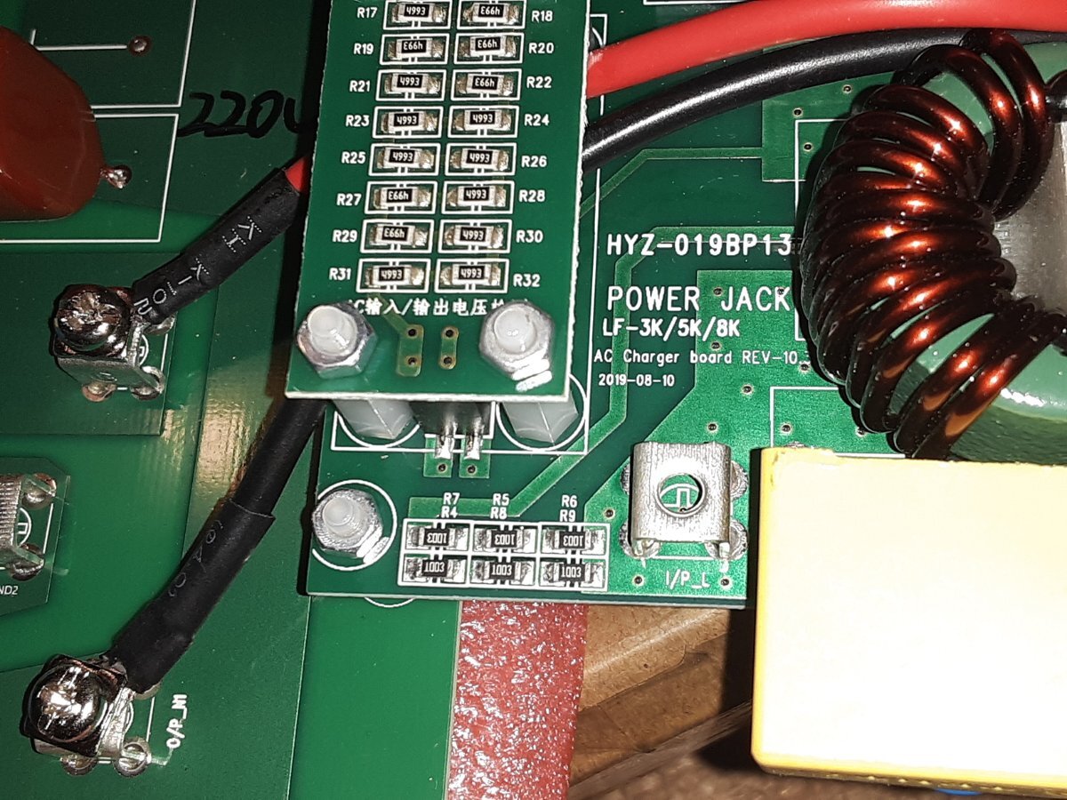
- SW1 is basically an adjustable resistor divider that varies the loading on the E124-LF-L transformer. The bigger the load (i.e. the more switches "on"), the more load it requires for the software shutdown threshold to be exceeded. (It also adjusts the "charge" current.)
- No. PJ's "split phase" design still runs 120v into the inverter (it will only work at 120v charge, you can't input 240v), and the other transformer phase is basically hardwired to the output terminals with no filtration. You might want to put another polyester cap on the unfiltered phase...
- Not unless PJ will give it to you. Such items are their IP (intellectual property), and it's up to them if they choose to divulge it. That being said, I can almost guarantee you that they will not hand it out.
- Ditto.
- RY01 is an SPST relay. PJ inverters cannot handle split-phase AC input; trying to connect split-phase AC input (or ground-bonded neutral) to the inverter is guaranteed to result in inverter failure. Additionally, as mentioned above, PJ "split phase" can only accept 120v AC input (and even then has a reputation for blowing FETs.)
Will have to dig into the connector pinout later--as swapping 2 pins is almost guaranteed to result in spectacular FET failure. If you wanted one of PJ's cheeky adapters, you'd need to get that from PJ; we at Genetry Solar don't have those. There aren't "updated" mainboards with a different connector AFAIK--no, PJ just uses a cheeky adapter.
Main board HYZ-002BP13, CN02 Pin=colors
Spending a few minutes with a DMM, and knowing that the FETs form an H-bridge results in the following pinout chart:
(L = left side, R = right side)
- VBAT+
- VBAT+
- R_FET_LG [low side Right MOS, Gate terminal]
- L_FET_HG [low side Left MOS, Gate]
- R_FET_HS [high side Right MOS, Source] - also "transformer line"
- L_FET_HS [low side Left MOS, Source] - ditto
- R_FET_HG [high side Right MOS, Gate]
- L_FET_LG [low side Left MOS, Gate]
- GND (VBAT-)
- GND (VBAT-)
A quick look at the above pinout shows that the FET drive signals are literally interleaved (like I've said elsewhere) in the worst possible way in the cable. Putting opposing signals side-by-side in a ribbon cable is ASKING for signal crosstalk (especially considering that large numbers of FETs in parallel will require a significant current--in the order of several amps--to switch on and off quickly)...
As to the voltage levels of said pins: this connector basically provides battery voltage (to run the control board) as well as the Source/Gate connections to each of the 4 MOS blocks ("boards") in the H-bridge. Low-side FETs' "Source" terminals are wired to battery negative, so the pairs are x_FET_LG / VBAT-. High-side FETs' control pairs are x_FET_HG / x_FET_HS. The maximum voltage range on the control pairs is +/-20v (or whatever the FETs' gate voltage specifications are).
Cross-checking a v9 board's FET connections to LF Driver board connections -> translating to a v11 board's connector pinout results in the following chart:
LEFT COLUMN: PINOUT AT MAINBOARD! Right Column: CN1_3 / CN1_4 on v11 control board (going with your "pin 1" guess, as it really isn't marked):
CN1: 1 -> CN1_3: 1 {BAT+}
CN1: 2 -> CN1_3: 2 {BAT+}
CN1: 3 -> CN1_3: 3 [LF Driver board Q03/Q05] {R_FET_LG}
CN1: 4 -> CN1_3: 6 [LF Driver board U1 6-7] {L_FET_HG}
CN1: 5 -> CN1_3: 8 [LF Driver board U2 5] {R_FET_HS}
CN1: 6 -> CN1_3: 5 [LF Driver board U1 5] {L_FET_HS}
CN1: 7 -> CN1_3: 7 [LF Driver board U2 6-7] {R_FET_HG}
CN1: 8 -> CN1_3: 4 [LF Driver board Q09/Q08] {L_FET_LG}
CN1: 9 -> CN1_3: 9 {BAT-}
CN1: 10 -> CN1_3: 10 {BAT-}
I do not think the pinout ascertained from a YT video is correct. Keep in mind that PJ ran the XHB-10 connector directly to an IDC connector, then mirrored the pinout into the mainboard connector with a 2x5 header.
Thanks you so much. I will review, try implementing this weekend and see if I can get everything working on my
u-Power ( Super-Power )
Model: LFPSW-10000-200 ; Low Frequency Pure Sine Wave “10,000” watt inverter with 200 Amp battery charger
It has all “Power Jack” Boards.