PLEASE NOTE: If you had an account with the previous forum, it has been ported to the new Genetry website!
You will need to reset the password to access the new forum. Click Log In → Forgot Password → enter your username or forum email address → click Email Reset Link.
Hi all!
ok. So, I ordered a pj inverter on ebay (don't shoot me, it was before I even knew about gs inverters), and now I'm starting to get concerned with reliability. The unit I purchased is a 6kw (yeah I know. More like 3) and I'm wondering if anyone can suggest the necessary changes to make it a decent inverter. I understand they do have a lot of potential, but just aren't built that well. So, what are some things I can swap out to fix it? Sean was saying that gs is kinda getting away from pj support now, but for the moment I'm going to assume that it's NOT one of the latest units, so I'm hopeful I can change out control boards etc with gs ones. At very least, maybe change out the filter caps if they're the small ones. New to this type of inverter, but I'm quite comfortable working on these types of things. Any help is appreciated!
Hi all!
So the GS project kinda got started by trying to improve the PJ inverter design. Long story short...after working our way systematically through the unearthed issues, we have ended up with a completely new design. You may be able to Band-Aid around some PJ issues...but at the end of the day, they can't be ignored.
PJ LF driver is a "typical Chinese LF driver circuit" (amazing that ALL LF Chinese inverter designs that I have seen use this exact same design)...consisting of (2) TLP350 opto FET drivers (for the high side FETs), and (2) totem pole transistor drivers (low side FETs). Right off the bat, we have imbalanced drivers...but this problem is significantly exacerbated by the power supply running the TLP350s at 18v, and the totem pole drivers at 12v and 10v (thanks to an LED on one of their inputs!) Part of the saving grace of this driver is that it is too weak to cleanly drive the FETs--and thus avoids a LOT of issues by simply being very poor. The rounded drive edges prevent "slamming" the transformer into the power supply rails, reducing internal EMI...but that's about the only plus side 😉. One significant result of the FETs not being cleanly switched, is that they are very vulnerable to blowing out at high loads due to not being fully "on". Heaven help you if the transformer primary ends up having more resistance than the FETs (due to not being fully turned on).
The weak LF driver results in FETs that generate a lot of heat (due to being poorly driven)--so PJ's solution is to decrease the transformer ratio (i.e. more input voltage required for the same output voltage). This results in the output wave flattening into a square wave with any significant load--but because the FETs are not switching in the mid part of the wave (out of headroom, 100% duty cycle), the "hot FET problem has been solved."
We can't forget the CPU firmware, either. Not only does the SPWM voltage regulation have no hysteresis (always +1 / -1 on the throttle--resulting in severe regulation oscillations), causing one bank of FETs to be run harder than the other--the dead time is too low for the weak LF driver. I was able to reduce no-load current on a PJ inverter simply by increasing the CPU's dead time setting--but this means that the FETs are constantly shorting out the DC input via H-bridge cross-conduction...which isn't good for their longevity.
The current GS control boards are pin-compatible with the PJ mainboards--but after finding significant fatal flaws with the design (the GS 12kw inverter design has had to be temporarily shelved due to these issues, until we prototype our own mainboards), the decision was made to sever compatibility with the PJ design. The issues start with the ribbon cable (far too thin for the gate capacitance, worst possible pinout for avoiding signal crosstalk--and I do mean worst!), and end with the PCB layout.
With all that in mind, there are 2 things that you can do to sorta help the PJ inverter designs. One is to make sure that there are no less than 2 full turns of wire (3 passes through the center) around the toroid on the transformer primary. This alone should significantly reduce no load current.
A second is to knock an LED off the control board. On a Rev. 10.x board, it's specifically LED4, directly above an LM339 (with RA3 next to it). (This LED is responsible for reducing the FET drive voltage for ONE quadrant from 12v to 10v.) This may quiet the transformer's hum down a little. (It's truly amazing to swap a GS control board into a PJ inverter--the tranny goes almost dead silent, assuming there's enough headroom for a pure sine output.)
I did provide PJ with an updated LF Driver design that's pin-compatible with their inverters; however, it reportedly results in FETs blowing at higher loads...despite simply being a full matched set of (4) TLP350 drivers with matched drive voltages (12v). Apparently I need to prototype it, and run some tests on my bench to see what's going on...issues could go from inductive spikes in the ribbon cable punching through the FET gates, or it could be signal crosstalk killing them across the battery input.
Yeah I think I saw a video with a guy wrapping the input lead 3 times around.... something, then into the primary rail and just doing that took it from like a 4A draw to a 0.3A draw or something like that at idle. Wish I could find that stupid video again but it seems to have evaporated.
Now, as far as this ribbon cable... I know in computer, and audio signals, cross-talk in wiring can be greatly reduced by simply twisting or braiding your wires rather than running them beside each other. If a fella were to make up his own heavier harness and replace the old ribbon with the new twisted harness, could that help in this case?
The led. Just literally remove it and done? Do I need to bridge any oc's left by removing it?
Am I able to do this control board swap for a gs one? It's a 6kw, 24v. No LCD, no outside v-adjustment (if the pics are even accurate of course).
I'll have more details and pictures once it arrives. It does say new, but my luck, it'll be new old stock. I dunno, we'll see.
Thank you for your help so far! ☺
10 hours ago, Glenn S said:Yeah I think I saw a video with a guy wrapping the input lead 3 times around.... something, then into the primary rail and just doing that took it from like a 4A draw to a 0.3A draw or something like that at idle.
I've done a lot of experiments with transformer chokes...much over 2 full turns (3 times through the center of the choke) doesn't seem to help anything...at least until the DC voltage is raised. Overdoing it doesn't hurt anything though. If you plan to run the inverter at higher input voltages, more turns/chokes are beneficial.
10 hours ago, Glenn S said:The led. Just literally remove it and done? Do I need to bridge any oc's left by removing it?
EDIT: Yes to the first, and NO necessary bridging. I just grab a needlenose pliers and break the LED off the board.
Yes. Since the low-side FETs are driven by a totem pole transistor setup, the output cannot go past the input. They have a pullup resistor being the only "on" signal...and they're pulled "low" by an open-drain LM339. Now, what about hanging an LED from that pullup resistor to +12v? (Reduces the "on" to 10v.)
10 hours ago, Glenn S said:Am I able to do this control board swap for a gs one?
Sorta yes, only with the current Rev. A.1 and Rev. B boards--which we admittedly don't have many extras of. We plan to offer Rev. C inverter board kits for DIYers who want to make their own inverter (more or less), but it will not be compatible with the PJ mainboards.
10 hours ago, Glenn S said:Now, as far as this ribbon cable... I know in computer, and audio signals, cross-talk in wiring can be greatly reduced by simply twisting or braiding your wires rather than running them beside each other. If a fella were to make up his own heavier harness and replace the old ribbon with the new twisted harness, could that help in this case?
We have tried all of the above in attempts to get the PJ mainboards to work...twisted pairs...separately shielded signal pairs...heavier gauge wire (22AWG instead of 28AWG ribbon cable)...chokes on the signal pairs (and combinations of those to boot). They help to some extent--pushing the "max limit" of the mainboard higher and higher--but at the end of the day, it appears that a large part of the fatal crosstalk fault is with the PCB trace layout of the mainboard itself.
Interestingly enough in test data gathered between the "mid-size" and "large" PJ mainboards, the "mid-size" seems to do significantly better than the "large" size in high wattage tests (>6kw). The only correlation I can make from that is the length of the signal pair crossing "no man's land" on the PJ mainboards...it's significantly longer on the "large" mainboard.
Think about it: if you put a (comparatively) low voltage/low current signal trace literally completely parallel with the entire length of a high voltage, very high amperage power plane (which runs in the opposite polarity)...what possibly could go wrong? For low wattage systems, it works alright. Higher wattage...umm.......not so much.
Thank you so much for all the info! Guess that's it for now and I'll be back when it arrives ☺
On 5/30/2021 at 1:13 PM, Sid Genetry Solar said:I've done a lot of experiments with transformer chokes...much over 2 full turns (3 times through the center of the choke) doesn't seem to help anything...at least until the DC voltage is raised. Overdoing it doesn't hurt anything though. If you plan to run the inverter at higher input voltages, more turns/chokes are beneficial.
EDIT: Yes to the first, and NO necessary bridging. I just grab a needlenose pliers and break the LED off the board.
Yes. Since the low-side FETs are driven by a totem pole transistor setup, the output cannot go past the input. They have a pullup resistor being the only "on" signal...and they're pulled "low" by an open-drain LM339. Now, what about hanging an LED from that pullup resistor to +12v? (Reduces the "on" to 10v.)
Sorta yes, only with the current Rev. A.1 and Rev. B boards--which we admittedly don't have many extras of. We plan to offer Rev. C inverter board kits for DIYers who want to make their own inverter (more or less), but it will not be compatible with the PJ mainboards.
We have tried all of the above in attempts to get the PJ mainboards to work...twisted pairs...separately shielded signal pairs...heavier gauge wire (22AWG instead of 28AWG ribbon cable)...chokes on the signal pairs (and combinations of those to boot). They help to some extent--pushing the "max limit" of the mainboard higher and higher--but at the end of the day, it appears that a large part of the fatal crosstalk fault is with the PCB trace layout of the mainboard itself.
Interestingly enough in test data gathered between the "mid-size" and "large" PJ mainboards, the "mid-size" seems to do significantly better than the "large" size in high wattage tests (>6kw). The only correlation I can make from that is the length of the signal pair crossing "no man's land" on the PJ mainboards...it's significantly longer on the "large" mainboard.
Think about it: if you put a (comparatively) low voltage/low current signal trace literally completely parallel with the entire length of a high voltage, very high amperage power plane (which runs in the opposite polarity)...what possibly could go wrong? For low wattage systems, it works alright. Higher wattage...umm.......not so much.
Hey Sid?
I was never able to find that video again with the choke. Any way you can show me in a pic how to do this? I mean, the process is easy. Not that. But, what do I wrap it around? Is there something I can grab online? I know it comes on off the battery input before the primary, then it gets looped 2 or 3 turns, then back into the primary rail. But wrapped through, or around what, I don't remember. What is the specific part, and I'll go buy It lol😃
Hey Sid?
Should just be the existing choke. PJ just has one full turn around the choke...and the wires are usually long enough to force a second turn around the same choke. Amazing how much that helps.
After reading comments and threads on TheBackshed.com, I personally bought a larger ferrite core ("split bobbin")...but did not find any significant gain over using it vs the stock PJ toroid choke.
Here's a photo of an inverter on my test bench with 2 full turns around the stock ferrite core. Your inverter will have at least one of these, as you'll see an easy 5A+ no-load current without one. PJ only does 1 full turn, which reduces no-load to ~1.5A. You should be able to get just under 1A with 2 full turns.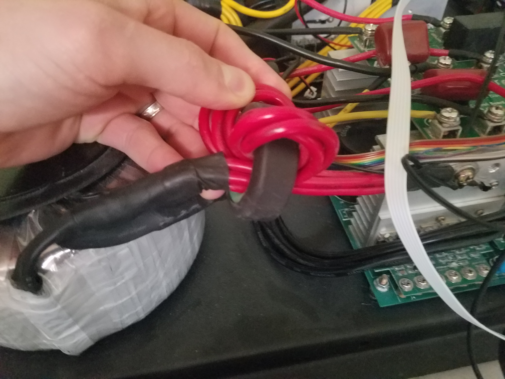
Sid, thank you so much! Inverter is set to arrive on Monday and the first thing I'm doing is voiding my warranty!
I'll do your other suggestions as well, while I have it open. You guys are awesome! Thanks again! Let ya know how she goes lol
Sid, thank you so much! Inverter is set to arrive on Monday and the first thing I'm doing is voiding my warranty!
It's a PJ, what warranty? 🤣😆
Feel free to move this thread to the u-power section if you want. Lol that's what showed up.
Anyway, it showed up in great condition, despite my concern with the damaged box it arrived in lol
Anything jump out at you off the hop? Just came back here to read where that led is again. Going to read back, then remove it lol
I also see an extra fan header so I'll add some more cooling by the transformer soon too.
Oh wait... This is a version 11 board. Led still in same place?
<a class="ipsAttachLink ipsAttachLink_image" data-fileext="jpg" data-fileid="425" href="/monthly_2021_06/535026864_2021-06-0718_53_01.jpg.f62a2b166288c9a1561e782fae6ef684.jpg" rel=""><img alt="2021-06-07 18.53.01.jpg" class="ipsImage ipsImage_thumbnailed" data-fileid="425" data-ratio="50" style="height:auto;" width="1000" data-src="//content.invisioncic.com/g308908/monthly_2021_06/1078690268_2021-06-0718_53_01.thumb.jpg.49bc644bcec1ac42007573dd3caaa3fe.jpg" src="/applications/core/interface/js/spacer.png" />
<a class="ipsAttachLink ipsAttachLink_image" data-fileext="jpg" data-fileid="426" href="/monthly_2021_06/1977020130_2021-06-0718_53_29.jpg.8336c7eb8933cd06cc08381c57e4a613.jpg" rel=""><img alt="2021-06-07 18.53.29.jpg" class="ipsImage ipsImage_thumbnailed" data-fileid="426" data-ratio="200" style="height:auto;" width="375" data-src="//content.invisioncic.com/g308908/monthly_2021_06/503918527_2021-06-0718_53_29.thumb.jpg.aecbd5f638f4b08106685016f2a9019b.jpg" src="/applications/core/interface/js/spacer.png" />
<a class="ipsAttachLink ipsAttachLink_image" data-fileext="jpg" data-fileid="427" href="/monthly_2021_06/453282352_2021-06-0718_53_53.jpg.ac5307c2779fc879fd58f91a9f48424e.jpg" rel=""><img alt="2021-06-07 18.53.53.jpg" class="ipsImage ipsImage_thumbnailed" data-fileid="427" data-ratio="200" style="height:auto;" width="375" data-src="//content.invisioncic.com/g308908/monthly_2021_06/422766855_2021-06-0718_53_53.thumb.jpg.159e9adb4e5768dbece073a18212029c.jpg" src="/applications/core/interface/js/spacer.png" />
47 minutes ago, Glenn S said:I also see an extra fan header so I'll add some more cooling by the transformer soon too.
Might be careful with that; the fans plugging directly into the board run off the 12v power supply--which I don't think can run 2 fans. (PJ "solves" this by using a thermal relay wired directly to battery voltage.)
V11...whoop-de-do. Adds a "charger amp limit" circuit, and upgrades the fan FET from a tiny SOT-23 SMT FET to a TO-220. That's about it. I can't clearly see from the photos, but betcha the LED is in the same place. I'd suggest testing the inverter before and after removing the LED, as a benchmark.
Oh wait... This is a version 11 board. Led still in same place?
I see the 3 ribbon cables of the 10.3 control board is gone . The v 11 board use bigger wires where the ribbon connecters is . Maybe the v 11 board is better .
The LF driver look like the same rev 9.0 on the 10.3 board . The LF driver need to be fix for the 20kw and 25kw and 30kw PS inverters . A bad LF driver will
destroy the mofetts and the 10.3 control board ( sound like firecrackers ) .
8 hours ago, Sid Genetry Solar said:Might be careful with that; the fans plugging directly into the board run off the 12v power supply--which I don't think can run 2 fans. (PJ "solves" this by using a thermal relay wired directly to battery voltage.)
V11...whoop-de-do. Adds a "charger amp limit" circuit, and upgrades the fan FET from a tiny SOT-23 SMT FET to a TO-220. That's about it. I can't clearly see from the photos, but betcha the LED is in the same place. I'd suggest testing the inverter before and after removing the LED, as a benchmark.
Oh ok, thanks for the heads up! I'll use 24v case fans and run them off the main input and then I shouldn't have to worry about that since they won't even be part of the internal system.
Sid, I cannot find this led anywhere! I see led2 which is lit up at the back panel, led5 in the middle of the board, and an unlabeled one lit up on the edge of the board.
And the 2 transistors on the control board... One is heatsinked, the other is not. That an oversight or design?
Idle draw is about .9A right now, but that is with transfer switch in the system.
On the plus side, it ran my microwave and my 15k BTU ac plus it started my compressor. So at least it works at this point lol
I see the 3 ribbon cables of the 10.3 control board is gone . The v 11 board use bigger wires where the ribbon connecters is . Maybe the v 11 board is better .
Nope, same cables used on PJ boards from v4 at least all the way 'till now. Ribbon cable for FET signals, and XHB for front panel/temp sensors.
The LF driver look like the same rev 9.0 on the 10.3 board . The LF driver need to be fix for the 20kw and 25kw and 30kw PS inverters . A bad LF driver will
I tried making 'em a better LF Driver board, but it reportedly results in instant FET blowups >9kw loads. PJ inverters are quite a song and dance it seems...I left it at that.
Sid, I cannot find this led anywhere! I see led2 which is lit up at the back panel, led5 in the middle of the board, and an unlabeled one lit up on the edge of the board.
They might've removed it already, which would be quite dandy. It'd be right near the LM339 next to the LF Driver board.
And the 2 transistors on the control board... One is heatsinked, the other is not. That an oversight or design?
The heatsinked FET runs the main power supply transformer; I hold that if they used a better (i.e. lower resistance) FET, they could mount it to the PCB easy.
The other FET switches the fans on and off--microscopic loads by comparison.
Thank you so much for all the great info! I'll look again for that led after work.
If you're game, I have 2 more questions. Then I'll leave you be until something breaks lmao...
First, upon testing, I see that she's putting out 115.9v steady on L1, but L2 kinda bounces all over between 110 and 113v. Anything I can do to clean that up even a little?
Second, can you tell me (not that I plan on playing with them unless it's necessary) which voltage adjuster controls which, input and output voltage?
Thanks again!